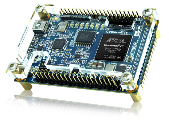
Terasic DE0-Nano
 |
FPGA | MIPS bitstream | RISCV bitstream |
| Altera Cyclone IV EP4CE22F17C6N |
de0nano_mips_100mhz.sof |
de0nano_riscv_100mhz.sof |
User manual: de0_nano_user_manual_v1.9.pdf
Quartus project directory: https://github.com/f32c/f32c/blob/master/rtl/proj/altera/de0_bram
Top-level module: https://github.com/f32c/f32c/blob/master/rtl/altera/de0_toplevel_bram.vhd
I/O pin enumeration
| Arduino | 0 | 1 | 2 | 3 | 4 | 5 | 6 | 7 |
|---|---|---|---|---|---|---|---|---|
| DE0 | btn_right | btn_left | ||||||
| Arduino | 8 | 9 | 10 | 11 | 12 | 13 | 14 | 15 |
| DE0 | LED #0 | LED #1 | LED #2 | LED #3 | LED #4 | LED #5 | LED #6 | LED #7 |
| Arduino | 16 | 17 | 18 | 19 | 20 | 21 | 22 | 23 |
| DE0 | switch #0 | switch #1 | switch #2 | switch #3 | ||||
| Arduino | 24 | 25 | 26 | 27 | 28 | 29 | 30 | 31 |
| DE0 |